-5V, -3V, How is the Negative Voltage Generated? Attached Circuit Analysis and Scheme

Negative Voltages are more important than you think! So here is how to make them! EB#52
Ⅰ. The principle of generating circuit diagram of negative voltage
We frequently need to employ negative voltages in electronic circuits. For instance, we frequently need to create a negative voltage for him when we employ op amps. Here is a straightforward illustration of his circuit from a positive 5V voltage to a negative 5V voltage.
I normally choose to utilize a specific negative voltage generation chip, such as the ICL7600, LT1054, and so forth, when I need to use negative voltage, however these chips are very expensive. Oh, I nearly completely overlooked the MC34063. The most usage is of this chip. I won't go into detail about the information found in the datasheet regarding the 34063's negative pressure producing circuit. Let's take a look at the two types of negative pressure generating circuits that we commonly use in single-chip electronic circuits.

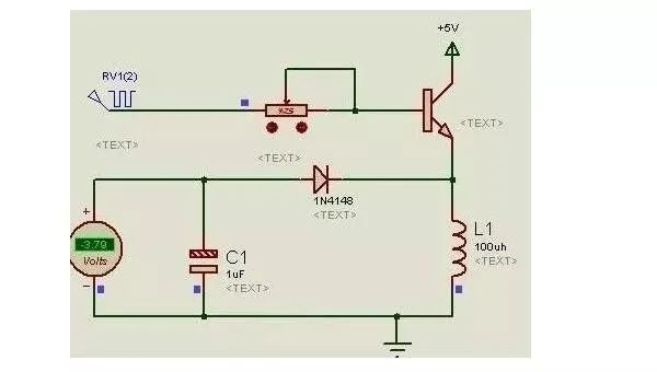
Figure. 1
PWM output is currently present in many single-chip microcomputers. PWM is frequently ineffective when we utilize a single-chip microcomputer. It is a wise decision to employ it to help create negative pressure.
One of the simplest circuits for producing negative voltage is the one shown above. He uses the least of the originals. It's very easy to do; all we need to give him is a square wave at roughly 1 kHz. It should be noted that this circuit has a very low generation load capacity, and the voltage drop after adding the load is also quite substantial.
The following circuit is produced for the above reasons:

Figure. 2
Ⅱ. Analysis of Negative Voltage Generation Circuit
Voltage is a physical quantity that represents the energy difference of a unit charge in an electrostatic field due to various potentials. It is sometimes referred to as potential difference or potential difference. The effort a unit positive charge must perform to move from point A to point B due to the force of the electric field determines its magnitude, and the direction of the voltage is described as travelling from high potential to low potential.
Simply explained, the voltage is the difference between potentials with respect to a reference point at a certain location. E - E parameter equals V. Typically, we use the negative pole of the power source as our point of reference. The voltage of the power source is Vcc=E power positive - E power negative.
Simply allow it to have a lower potential in relation to the negative pole of the power supply if you wish to generate a negative voltage. Another power source must be involved for the cost to be reduced. The basic idea is to link two power supply in series with one another. The reference power supply 1's negative pole and the power supply 2's positive pole are connected in series. The negative voltage is present at power supply 2's negative terminal.

Figure. 3
A circuit that produces negative voltage: By charging the capacitor, a new power source is equivalently created. The capacitor becomes comparable to power supply 2 once it is linked in series with GND. There is a negative voltage produced.

Figure. 4
1. Capacitor charging: The charging circuit is VCC-Q2-C1-D2-GND, and when PWM is low, Q2 is turned on, Q1 is turned off, and VCC charges C1 through Q2. Right negative and left positive on C1.

Figure. 5
2. The charge on Capacitor C1 is complete.

Figure. 6
3. The high potential pole of the capacitor C1 is linked in series with the reference point. C1 serves as the power source. A negative voltage results from C1 discharging and freewheeling from C2.
Q2 is switched off, Q1 is turned on, and C1 starts to discharge when the PWM is low. C1-C2-D1 is the discharge loop, and C2 is actually being charged during this operation. The bottom of C2 is positive and the top is negative once it has been fully charged. The voltage of -5V can be output if the VCC potential is 5:00 volts.

Figure. 7
Ⅲ. Scheme for generating negative voltage (-5V)

Figure. 8
The output capability of 7660 and MAX232 is limited, and it is very difficult to make an oscilloscope with a high-speed op amp, so Wei Kun also has to use 4 slices in parallel to expand the current.
The first version is 7660 two in parallel.
Ordinary DC/DC chips can produce negative voltage, and they do it with accuracy equal to that of positive voltage. In addition, they have a very high driving capability that can reach more than 300mA.
The generic switching power supply chip has a negative voltage generation capability. The switching power supply's PWM output cannot be used to drive the charge pump at all. Additionally, it has a relatively low cost and can produce a huge current. The necessary amount of ripple is unknown to me. The ripple is fairly tiny after LC filters the charge pump. Because the 7660 is a charge pump, the current is really low.
How should the digital ground and the analog ground be handled? The +5V of the digital power supply and the +5V of the analog power supply are powered separately in the design of the complete oscilloscope.
The analog ground and the digital ground must be connected in order for the circuit to function.
The two grounds should be joined together at a stable ground reference since the ground return current of the digital part cannot pass through the analog part.
Ⅳ. The meaning of negative voltage
1. Rules created by humans. For instance, the telephone system is powered by -48V, preventing galvanic corrosion of the telephone line. Of course, answering the phone backwards is also an option; all that is required is a modification in the voltage reference point.
2. The interface for communication is necessary. For instance, negative voltage is required for the RS232 interface. -3V15V equals 1, and +3V+15V equals 0. When the communication interface was first created, this protocol was used, and it can only be adhered to. PS: Interface chips with their own charge pumps and the ability to produce negative voltage include those like the MAX232.
3. Give (non-rail-to-rail) op amps electricity rails. Rail-to-rail input/output capabilities are not available in traditional op amps like the OP07. The output voltage range is always 2V lower and the input voltage range is always 1V lower than the power supply voltage range. This means that if VEE uses 0V, the input voltage must be greater than 1V and the output voltage cannot be less than 2V. Some requirements for circuit design might not be met in this situation. It is necessary to provide the op amp with a negative voltage, such as -5V, in order for the op amp to function normally under input/output situations close to 0V. But as rail-to-rail op amps gain prominence, this circumstance is fading away.
4. This one has a self-destructing circuit and Chinese traits. Generally speaking, the chip's internal safety circuit is not well-protected against negative voltage, thus the chip can be successfully destroyed as long as the current is somewhat higher and a low negative voltage is not required.
1. How to detect negative voltage current?
The same as the positive voltage and current measurement method, connect the ammeter in series to the circuit to be measured, the difference is that the polarity of the ammeter is reversed.
2. How is the negative voltage in the power supply generated?
In fact, the power supply does not have positive and negative, it is a problem of setting the reference point. A power supply of 5V, with the negative pole as the reference "zero point", the positive pole is +5v; with the positive pole as the reference "zero point", the negative pole is -5V.
3. What is the difference between negative voltage and negative potential?
A point in the circuit is set as the reference point, and the potential of the reference point is zero. For example, the earth is set as the reference point for ~ 220V, and the chassis is set as the reference point for general instruments.
The voltage value of a point to the reference point is the potential of that point. Such as Va, Vb.
Voltage is the potential difference like Uab = Va - Vb.
Negative potential means that the voltage of the point to the reference point is negative. For example, the positive electrode of a 3V battery is grounded, and the negative electrode potential is - 3V.
Negative voltage means that the potential difference between two points is negative. Such as Uab = -6V, it means Vb is 6V higher than Va.
 Discovering New and Advanced Methodology for Determining the Dynamic Characterization of Wide Bandgap DevicesSaumitra Jagdale15 March 20242180
For a long era, silicon has stood out as the primary material for fabricating electronic devices due to its affordability, moderate efficiency, and performance capabilities. Despite its widespread use, silicon faces several limitations that render it unsuitable for applications involving high power and elevated temperatures. As technological advancements continue and the industry demands enhanced efficiency from devices, these limitations become increasingly vivid. In the quest for electronic devices that are more potent, efficient, and compact, wide bandgap materials are emerging as a dominant player. Their superiority over silicon in crucial aspects such as efficiency, higher junction temperatures, power density, thinner drift regions, and faster switching speeds positions them as the preferred materials for the future of power electronics.
Read More Applications of FPGAs in Artificial Intelligence: A Comprehensive GuideUTMEL29 August 2025527
This comprehensive guide explores FPGAs as powerful AI accelerators that offer distinct advantages over traditional GPUs and CPUs. FPGAs provide reconfigurable hardware that can be customized for specific AI workloads, delivering superior energy efficiency, ultra-low latency, and deterministic performance—particularly valuable for edge AI applications. While GPUs excel at parallel processing for training, FPGAs shine in inference tasks through their adaptability and power optimization. The document covers practical implementation challenges, including development complexity and resource constraints, while highlighting solutions like High-Level Synthesis tools and vendor-specific AI development suites from Intel and AMD/Xilinx. Real-world applications span telecommunications, healthcare, autonomous vehicles, and financial services, demonstrating FPGAs' versatility in mission-critical systems requiring real-time processing and minimal power consumption.
Read More Xilinx FPGAs: From Getting Started to Advanced Application DevelopmentUTMEL08 September 20259
This guide is your comprehensive roadmap to understanding and mastering the world of Xilinx FPGA technology. From selecting your first board to deploying advanced AI applications, we'll cover everything you need to know to unlock the potential of these remarkable devices. The global FPGA market is on a significant growth trajectory, expected to expand from USD 8.37 billion in 2025 to USD 17.53 billion by 2035. This surge is fueled by the relentless demand for high-performance, adaptable computing in everything from 5G networks and data centers to autonomous vehicles and the Internet of Things (IoT). This guide will walk you through the key concepts, tools, and products in the Xilinx ecosystem, ensuring you're well-equipped to be a part of this technological revolution.
Read More Advanced CMOS Devices with Wide Bandgap and Ultrawide Bandgap TechnologiesSaumitra Jagdale15 March 20242885
Power and radio frequency electronics play an increasingly important role in energy-efficient and collaborative future as there is always a demand for faster, smaller, high-voltage and more conductive transistors. Traditionally, silicon has been the semiconductor of choice due to its extensive research and manufacturing history, and natural abundance. While silicon power devices continue to maximize performance, many applications are now integrating wider-band gap semiconductors. These materials offer a significantly higher voltage-conducting capacity, surpassing silicon's limits in tradeoffs related to ON-resistance, capacitances, and breakdown voltage.
Read More FPGA in Industry and Communication: Key Players, Technologies, and Future TrendsUTMEL07 March 20251052
FPGAs (Field Programmable Gate Arrays) have become the core hardware in the industrial and communication fields due to their programmability and parallel processing capabilities.
Read More
Subscribe to Utmel !
![ISD203XG]() ISD203XG
ISD203XGIsocom Components
![IS829SM]() IS829SM
IS829SMIsocom Components
![ILQ5XSMT&R]() ILQ5XSMT&R
ILQ5XSMT&RIsocom Components
![ISP847XASM]() ISP847XASM
ISP847XASMIsocom Components
![PS2502-4XSM]() PS2502-4XSM
PS2502-4XSMIsocom Components
![PS2502-2XSM]() PS2502-2XSM
PS2502-2XSMIsocom Components
![TIL196AX]() TIL196AX
TIL196AXIsocom Components
![TIL116XG]() TIL116XG
TIL116XGIsocom Components
![TIL114XSMT&R]() TIL114XSMT&R
TIL114XSMT&RIsocom Components
![TLP621-2GRSM]() TLP621-2GRSM
TLP621-2GRSMIsocom Components


